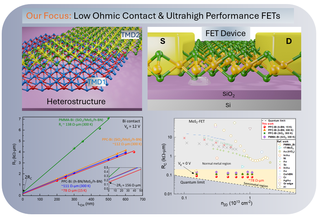
Achieving residual-free, ideal Ohmic contacts in vdW-layered semiconductors remains one of the most critical challenges in the field of 2D electronics. A universal Ohmic contact platform that functions effectively for both n-type and p-type vdW semiconductors remains an unresolved issue in the research community. To fully establish this contact platform, we aim to:
i) Develop an optimized tunneling barrier at the contact interface, which enables Ohmic behavior for both n-type and p-type vdW semiconductors,
ii) Design and fabricate high-mobility field-effect transistors (FETs) using vdW-layered semiconductors with the newly engineered Ohmic contacts, and
iii) Break the thermal threshold swing limit in both n-type and p-type 2D-FETs, enabling efficient low-power operation. If realized, this breakthrough will overcome one of the fundamental limitations in 2D semiconductor technology, bringing vdW-layered semiconductors closer to post-Si era electronics. By developing a universal Ohmic contact platform, our research could drive next-generation ultrafast, low-power transistors, offering high mobility and energy efficiency unmatched by conventional Si-based electronics. This work has far-reaching implications for future semiconductor industries, including flexible electronics, energy-efficient computing, and quantum device integration.

Copyright © 2025 Institute of Low-Dimensional Quantum Materials, Hubei University of Technology.